Eight nodes on one current-limited rail. Hard draw sags the rail; the sag is the ambient scalar every ADC feels at once. Fastest of the three to settle, most scope-legible — and the mechanism (droop control) is already grid-proven.
| Qty | Item | Notes |
|---|---|---|
| 8 | ESP32-S3 N16R8 (ESP32-S3-DevKitC-1 layout) | Lonely Binary / any DevKitC-1-layout S3; logic power SEPARATE from the shared rail (see warning) |
| 1 | bench supply, current-limited | e.g. 5 V @ 1–2 A limit; OR fixed supply + series R + cap bank |
| 1 | series resistor ~1 Ω / 5 W (if no CC supply) | creates the sag |
| 1 | cap bank 2200–4700 µF | smooths, slows the medium usefully |
| 8 | logic-level MOSFETs (e.g. AO3400 / IRLZ44N) | one load switch per node |
| 8 | load resistors ~22 Ω / 5 W | per-node draw on the shared rail |
| 16 | divider resistors (10 kΩ + 10 kΩ) | halve 5 V rail into 3V3-safe ADC range, one divider per node |
| — | bus wire / distribution board | every node ties to the SAME rail and common ground |
| Signal | ESP32 pin | Connects to |
|---|---|---|
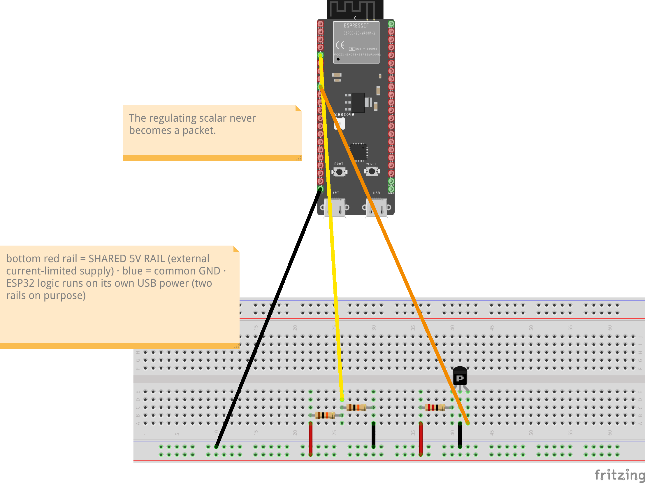
| Rail sense | GPIO 5 (ADC1) | midpoint of 10k/10k divider across rail → GND |
| Load PWM | GPIO 16 | MOSFET gate; drain → 22 Ω → rail; source → GND |
| GND | GND | common with rail ground |
Board (ESP32-S3-DevKitC-1 layout, N16R8): sense is GPIO 5 — on the S3, ADC1 = GPIO 1–10 (GPIO 5 = ADC1_CH4) and ADC1 doesn't fight WiFi. The classic-ESP32 GPIO 34 is not an ADC pin on the S3. On octal-PSRAM N16R8 leave GPIO 33–37 (PSRAM) and GPIO 26–32 (SPI flash) alone — touching them crashes the cache; safe GPIOs are 1–18, 21, 38–42, 47.
Per-node wiring, breadboard view — bottom red rail is the SHARED 5 V rail (external supply, deliberately not fed from the board), logic stays on USB; MOSFET drawn by pin name (D·S·G), check your package's datasheet. Pin positions are correct; the USB connector shown is cosmetic (micro-USB in the drawing vs the lab boards' dual USB-C). Editable sketch: lab2_rail_wiring.fzz
V_NOM   = 5.0          # firm-rail voltage
V_FLOOR = 4.5          # full-backoff point
# duty follows a droop line between the two — same law as grid governors

every 100 ms:                       # rail is a fast medium; loop fast
    v = read_rail_adc() * 2.0       # undo the divider
    duty = clamp((v - V_FLOOR) / (V_NOM - V_FLOOR), 0.0, 1.0)
    set_load_pwm(duty)
    # no node signals another. the sag already told everyone.
A multimeter or scope on the rail is the honest gauge — physically read-only by nature. For logging: one spare ESP32 with ONLY a divider tap, WiFi reporting is fine here (RF is not the medium), or wired serial for purity. Never give the gauge a load.
Scope screenshots of dip-and-recover are the money graphs. This is the lab to show an engineer first: droop control they already trust, one level down.